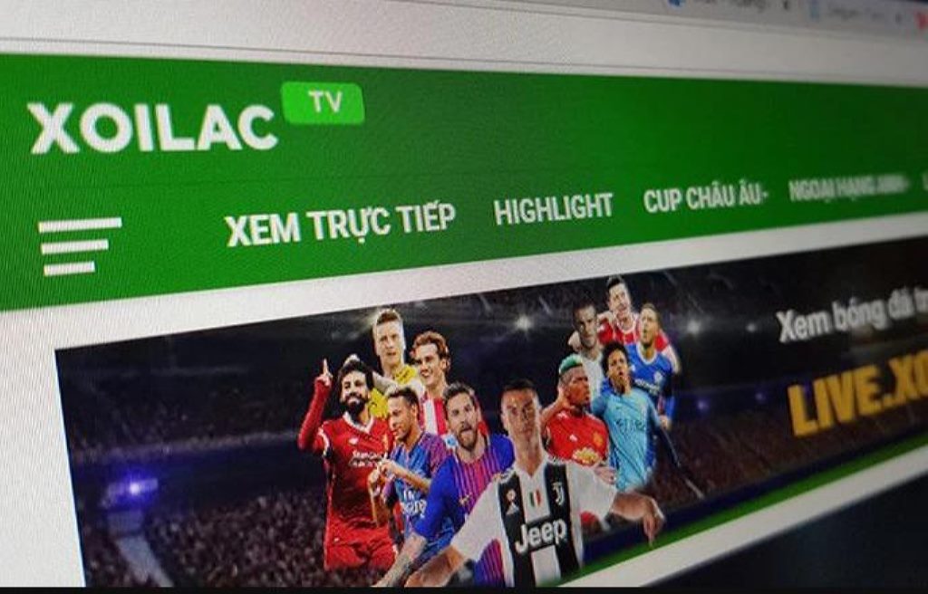
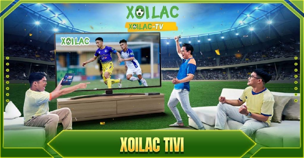
Xoilac TV – Kênh xem trực tiếp bóng đá hoàn toàn miễn phí
Bóng đá, môn thể thao vua, luôn là niềm đam mê của hàng triệu người trên thế giới, trong đó có Việt Nam. Để có thể theo dõi các trận đấu bóng đá yêu thích, người hâm mộ thường phải trả phí cho các nhà đài truyền hình. Tuy nhiên, với sự phát triển của công nghệ như hiện nay thì đã có vô số trang web, ứng dụng xem trực tiếp bóng đá miễn phí, chất lượng cao. Trong số đó, Xoilac TV là một trong những trang web được yêu thích nhất.
Mục tiêu phát triển của website trực tiếp bóng đá Xoilac TV
Mục tiêu phát triển của website truc tiep bong da Xoilac TV có thể được chia thành các mục tiêu cụ thể như sau:
Mong muốn trở thành một kênh xem bóng đá miễn phí
Đây là mục tiêu quan trọng nhất mà Xoilac muốn hướng tới. Trang web này cung cấp các link xem trực tiếp bóng đá miễn phí, chất lượng cao và ổn định. Xôi Lạc TV luôn nỗ lực để cải thiện chất lượng của các link xem trực tiếp, đồng thời mở rộng phạm vi cung cấp các trận đấu bóng đá.
Là kênh có hệ thống âm thanh và hình ảnh chất lượng
Xoilac TV luôn chú trọng đến chất lượng âm thanh, hình ảnh của các link xem trực tiếp. Trang web này sử dụng các công nghệ tiên tiến để đảm bảo rằng người xem có được trải nghiệm xem tốt nhất.
Giúp người dùng dễ dàng tiếp cận vào các kênh bóng đá
Xôi Lạc TV thiết kế giao diện thân thiện với người dùng, giúp người xem dễ dàng tìm kiếm và truy cập các link xem trực tiếp. Trang web này cũng có ứng dụng trên điện thoại di động, giúp người xem có thể theo dõi các trận đấu bóng đá mọi lúc, mọi nơi.
Những ưu điểm nổi bật của trang web trực tiếp bóng đá Xoilac TV
Những ưu điểm nổi bật của trang web trực tiếp bóng đá Xoilac TV bao gồm:
Không thu phí người xem
Xoilac cung cấp các link xem trực tiếp bóng đá miễn phí, không yêu cầu người xem phải đăng ký tài khoản hay trả bất kỳ khoản phí nào. Đây là một trong những ưu điểm nổi bật nhất của trang web này.
Giao diện website dễ sử dụng và đẹp mắt
Giao diện website của Xôi Lạc TV được thiết kế đơn giản, dễ sử dụng và đẹp mắt. Người xem có thể dễ dàng tìm kiếm và truy cập các link xem trực tiếp.
Phát sóng tất cả các giải bóng đá hàng đầu
Xoilac TV cung cấp các link xem trực tiếp của tất cả các giải bóng đá hàng đầu trên thế giới. Có thể kể đến như là Ngoại hạng Anh, La Liga, Serie A, Bundesliga, Champions League, Europa League,…
Cung cấp hệ thống link xem trực tiếp bóng đá hiện đại
Xoilac TV sử dụng các công nghệ tiên tiến để cung cấp các link xem trực tiếp chất lượng cao và ổn định. Người xem có thể thưởng thức các trận đấu bóng đá với hình ảnh sắc nét và âm thanh sống động.
Phát sóng trực tiếp bóng đá với chất lượng cao
Xôi Lạc TV được biết đến là một kênh bóng đá trực tuyến có chất lượng cao sẽ mang đến cho người xem trải nghiệm xem tốt nhất.
Tructiepbongda với tốc độ mượt mà
Tốc độ mượt mà cũng là một tiêu chí quan trọng không kém. Người xem không muốn phải chờ đợi quá lâu để xem được trận đấu. Một kênh bóng đá trực tuyến có tốc độ mượt mà sẽ giúp người xem có thể theo dõi các trận đấu một cách trọn vẹn.
Link trực tiếp bóng đá với bình luận cuốn hút
Bình luận viên đóng vai trò quan trọng trong việc tạo nên sự hấp dẫn cho các trận đấu bóng đá trực tuyến. Một kênh bóng đá trực tuyến có bình luận cuốn hút sẽ giúp người xem hiểu rõ hơn về trận đấu và cảm nhận được sự hồi hộp, kịch tính của trận đấu.
Kênh bóng đá trực tiếp không có quảng cáo
Quảng cáo có thể gây gián đoạn và ảnh hưởng đến trải nghiệm xem của người hâm mộ. Một kênh bóng đá trực tuyến không có quảng cáo sẽ giúp người xem có thể tập trung theo dõi trận đấu một cách trọn vẹn nhất.
Tất cả những tiêu chí trên đều được trang web Xôi Lạc TV đáp ứng đầy đủ. Xoilac TV là một trong những kênh bóng đá trực tuyến hàng đầu Việt Nam, cung cấp các link xem trực tiếp của tất cả các giải bóng đá hàng đầu trên thế giới với chất lượng cao, tốc độ mượt mà, bình luận cuốn hút và không có quảng cáo.
Hướng dẫn cách xem trực tiếp bóng đá
Để xem trực tiếp bóng đá tại Xôi Lạc TV, bạn có thể thực hiện theo các bước sau:
- Truy cập trang web Xoilac TV. Bạn có thể truy cập trang web Xôi Lạc TV bằng cách nhập địa chỉ trang web vào thanh địa chỉ của trình duyệt.
- Chọn trận đấu muốn xem. Tại trang chủ của Xôi Lạc TV, bạn sẽ thấy danh sách các trận đấu đang diễn ra hoặc sắp diễn ra. Nhấp vào trận đấu muốn xem để xem trực tiếp.
- Chọn link xem phù hợp. Xoilac cung cấp nhiều link xem trực tiếp cho mỗi trận đấu. Bạn có thể chọn link xem phù hợp với nhu cầu của mình, chẳng hạn như link xem chất lượng cao, link xem không có quảng cáo,…
- Chờ vài giây để video phát. Sau khi chọn link xem, bạn cần chờ vài giây để video phát. Nếu video không phát, bạn có thể thử đổi sang link xem khác.
Lưu ý:
- Để có trải nghiệm xem tốt nhất, bạn nên sử dụng kết nối internet có tốc độ cao và ổn định.
- Bạn có thể bật chế độ full màn hình để xem trận đấu với chất lượng tốt nhất.
- Nếu gặp vấn đề về chất lượng hình ảnh hoặc âm thanh, bạn có thể thử đổi sang một link khác.
Sau khi nhấp vào nút Xem trực tiếp, bạn sẽ được chuyển đến trang phát trực tiếp của trận đấu. Tại đây, bạn có thể xem trận đấu với chất lượng hình ảnh và âm thanh cao. Bạn cũng có thể tham gia bình luận với những người hâm mộ khác trên trang web.
Để xem trực tiếp bóng đá trên điện thoại di động, bạn có thể tải ứng dụng Xoilac TV về thiết bị của mình. Ứng dụng này có giao diện đơn giản và dễ sử dụng, tương tự như trên trang web.
Những lý do nên xem trực tiếp bóng đá
Xoilac TV là một trong những kênh bóng đá trực tuyến hàng đầu Việt Nam. Trang web này cung cấp các link xem trực tiếp của tất cả các giải đấu bóng đá hàng đầu trên thế giới với chất lượng cao, tốc độ mượt mà, bình luận cuốn hút và không có quảng cáo. Dưới đây là một số lý do nên xem trực tiếp bóng đá tại Xôi Lạc TV:
Chất lượng hình ảnh và âm thanh cao
Chất lượng hình ảnh và âm thanh cao là một trong những ưu điểm nổi bật của Xoilac. Trang web này sử dụng các công nghệ tiên tiến để cung cấp các link xem trực tiếp chất lượng cao và ổn định. Người xem có thể thưởng thức các trận đấu bóng đá với hình ảnh sắc nét, âm thanh sống động, chân thực như đang ngồi trên sân vận động.
Để đảm bảo chất lượng hình ảnh và âm thanh cao, Xoilac sử dụng các công nghệ sau:
- Công nghệ HD: Xoilac TV sử dụng công nghệ HD để cung cấp hình ảnh sắc nét, chân thực với độ phân giải Full HD (1920 x 1080 pixel).
- Công nghệ âm thanh vòm: Xoilac sử dụng công nghệ âm thanh vòm để mang đến cho người xem trải nghiệm âm thanh sống động, chân thực như đang ngồi trên sân vận động.
- Công nghệ chống giật lag: Xoilac sử dụng công nghệ chống giật lag để đảm bảo chất lượng hình ảnh và âm thanh ổn định, không bị gián đoạn.
Tốc độ mượt mà
Tốc độ mượt mà là một ưu điểm khác của Xoilac. Trang web này có hệ thống máy chủ mạnh mẽ, đảm bảo tốc độ mượt mà cho các link xem trực tiếp. Người xem có thể theo dõi các trận đấu một cách trọn vẹn, không bị giật lag, gián đoạn.
Để đảm bảo tốc độ mượt mà, Xoilac sử dụng các công nghệ sau:
- Công nghệ truyền tải dữ liệu tiên tiến: Xoilac sử dụng công nghệ truyền tải dữ liệu tiên tiến để đảm bảo tốc độ đường truyền ổn định, không bị gián đoạn.
- Công nghệ chống giật lag: Xoilac sử dụng công nghệ chống giật lag để đảm bảo chất lượng hình ảnh và âm thanh ổn định, không bị gián đoạn.
Bình luận cuốn hút
Bình luận cuốn hút là một trong những yếu tố quan trọng giúp Xoilac TV thu hút được đông đảo người hâm mộ. Trang web này có đội ngũ bình luận viên chuyên nghiệp, giàu kinh nghiệm, với khả năng truyền tải cảm xúc và phân tích kỹ thuật, chiến thuật sắc sảo.
Các bình luận viên của Xoilac TV có kiến thức bóng đá vững vàng, nắm bắt được các quy tắc, luật lệ, cũng như các chiến thuật, kỹ thuật của môn thể thao này. Họ có khả năng diễn đạt mạch lạc, rõ ràng, thu hút người nghe. Bên cạnh đó, các bình luận viên của Xoilac TV cũng có giọng nói truyền cảm, có khả năng truyền tải cảm xúc của trận đấu đến người nghe.
Không có quảng cáo
Không có quảng cáo là một trong những ưu điểm nổi bật của Xoilac TV. Trang web này không hiển thị bất kỳ quảng cáo nào, giúp người xem có thể tập trung theo dõi trận đấu một cách trọn vẹn nhất.
Quảng cáo có thể gây gián đoạn và ảnh hưởng đến trải nghiệm xem của người hâm mộ. Xoilac TV hiểu được điều này, vì vậy trang web đã quyết định loại bỏ hoàn toàn quảng cáo.
Việc không có quảng cáo cũng giúp Xoilac TV mang đến cho người xem trải nghiệm xem chất lượng cao hơn. Trang web có thể tập trung tối đa vào việc cung cấp các link xem trực tiếp chất lượng cao, không bị giật lag, gián đoạn.
Thông tin trận đấu
Xoilac cung cấp đầy đủ thông tin về các trận đấu như lịch thi đấu, kết quả thi đấu, bảng xếp hạng,… giúp người hâm mộ có thể cập nhật chính xác thông tin nhanh chóng.
Kết quả xổ số
Xôi Lạc TV cung cấp kết quả xổ số của tất cả các đài trên toàn quốc. Người hâm mộ có thể theo dõi kết quả xổ số một cách nhanh chóng và tiện lợi.
Tin tức thể thao
Xoilac TV cung cấp tin tức thể thao mới nhất trong nước và quốc tế. Người hâm mộ có thể cập nhật tin tức thể thao một cách nhanh chóng và đầy đủ.
Những lưu ý khi xem trực tiếp bóng đá tại Xoilac.TV
Xoilac.TV là một trong những kênh bóng đá trực tuyến hàng đầu Việt Nam. Trang web này cung cấp các link xem trực tiếp của tất cả các giải đấu bóng đá hàng đầu trên thế giới với chất lượng cao, tốc độ mượt mà, bình luận cuốn hút và không có quảng cáo. Tuy nhiên, khi xem trực tiếp bóng đá tại Xoilac.TV, cần lưu ý các vấn đề sau:
Sử dụng mạng kết nối ổn định
Kết nối internet là yếu tố quan trọng nhất quyết định chất lượng xem trực tiếp bóng đá tại Xoilac.TV. Nếu kết nối internet quá chậm, người xem có thể gặp phải tình trạng giật lag, thậm chí không thể xem được trận đấu. Do đó, người xem nên sử dụng kết nối internet có tốc độ cao và ổn định, ít nhất là 10Mbps.
Thử đổi sang một link khác nếu gặp vấn đề
Trong quá trình xem trực tiếp bóng đá, nếu gặp vấn đề về chất lượng hình ảnh hoặc âm thanh, người xem có thể thử đổi sang một link khác. Xoilac.TV thường cung cấp nhiều link xem trực tiếp cho mỗi trận đấu để đảm bảo người xem có thể xem được trận đấu với chất lượng tốt nhất.
Không nên tải xuống các ứng dụng hoặc phần mềm từ các trang web không uy tín
Một số trang web giả mạo Xoilac.TV có thể yêu cầu người xem tải xuống các ứng dụng hoặc phần mềm. Người xem không nên tải xuống các ứng dụng hoặc phần mềm từ các trang web không uy tín vì có thể chứa virus hoặc mã độc.
Cẩn thận với các thông tin giả mạo
Một số trang web giả mạo Xoilac.TV có thể đăng tải các thông tin giả mạo như kết quả trận đấu, lịch thi đấu,… Người xem nên kiểm tra thông tin từ các nguồn uy tín trước khi chia sẻ hoặc bình luận.
Tuyệt đối không tham gia các hành vi vi phạm pháp luật
Xoilac.TV là một trang web giải trí, không khuyến khích các hoạt động vi phạm pháp luật như cá cược, đánh bạc,… Người xem nên tuân thủ pháp luật và tránh tham gia các hoạt động trái phép.
Tuân thủ những lưu ý trên sẽ giúp bạn có trải nghiệm xem trực tiếp bóng đá tại Xoilac.TV một cách tốt nhất.
Xoilac TV – Trang web phát sóng trực tiếp bóng đá được yêu thích nhất hiện nay
Xoilac TV là một trong những kênh bóng đá trực tuyến hàng đầu Việt Nam, cung cấp các link xem trực tiếp của tất cả các giải đấu bóng đá hàng đầu trên thế giới với chất lượng cao, tốc độ mượt mà, bình luận cuốn hút và không có quảng cáo. Ngoài ra, Xoilac TV còn cung cấp nhiều tính năng tiện ích khác như:
Lịch thi đấu chính xác
Xoilac TV cập nhật lịch thi đấu của tất cả các giải đấu bóng đá hàng đầu trên thế giới một cách chính xác và đầy đủ. Điều này giúp người hâm mộ nắm bắt được lịch thi đấu của các đội bóng yêu thích, cũng như không bỏ lỡ bất kỳ trận đấu nào.
Bảng xếp hạng 247
Xoilac TV cập nhật bảng xếp hạng của tất cả các giải đấu bóng đá hàng đầu trên thế giới một cách nhanh chóng và chính xác. Điều này giúp người hâm mộ theo dõi được tình hình thi đấu của các đội bóng, cũng như dự đoán được kết quả của các trận đấu.
Kết quả bóng đá 24h
Xoilac TV cập nhật kết quả các trận đấu bóng đá một cách nhanh chóng và chính xác. Điều này giúp người hâm mộ nắm bắt được kết quả của các trận đấu đã diễn ra, cũng như có thể theo dõi lại các trận đấu đã qua.
Highlight bóng đá ghi lại khoảnh khắc
Xoilac TV cung cấp các video highlight ghi lại những khoảnh khắc đáng nhớ của các trận đấu bóng đá. Điều này giúp người hâm mộ có thể xem lại những khoảnh khắc đáng nhớ của trận đấu, cũng như có thể xem lại những pha bóng đẹp mắt.
Tin tức bóng đá hôm nay
Xoilac TV cập nhật tin tức bóng đá mới nhất trong nước và quốc tế. Điều này giúp người hâm mộ nắm bắt được những thông tin mới nhất về bóng đá, cũng như có thể thảo luận về các tin tức bóng đá với những người hâm mộ khác.
Tỷ lệ kèo trước trận
Xoilac TV cung cấp tỷ lệ kèo của các trận đấu bóng đá hàng đầu trên thế giới. Điều này giúp người hâm mộ có thể tham khảo tỷ lệ kèo trước khi đặt cược, cũng như có thể theo dõi tỷ lệ kèo của các trận đấu đang diễn ra.
Cẩm nang chính xác
Xoilac TV cung cấp các cẩm nang về bóng đá như luật bóng đá, lịch sử bóng đá,… Điều này giúp người hâm mộ có thể hiểu rõ hơn về môn thể thao vua, cũng như có thể nâng cao kiến thức về bóng đá.
Livescore 7m
Xoilac TV cung cấp thông tin về các trận đấu bóng đá đang diễn ra với thời gian cập nhật 7m một lần. Điều này giúp người hâm mộ có thể nắm bắt được diễn biến trận đấu một cách nhanh chóng và chính xác.
Câu hỏi liên quan Xoilac TV
Dưới đây là một số câu hỏi mà nhiều người xem thường thắc mắc liên quan đến Xoilac TV:
Xoilac TV là gì?
Xoilac TV là một trang web phát sóng trực tiếp bóng đá hàng đầu Việt Nam, cung cấp các link xem trực tiếp của tất cả các giải đấu bóng đá hàng đầu trên thế giới với chất lượng cao, tốc độ mượt mà, bình luận cuốn hút và không có quảng cáo.
Xoilac TV có tính phí không?
Không, Xoilac là trang web miễn phí. Người dùng có thể xem trực tiếp bóng đá trên Xoilac mà không cần đăng ký hoặc trả phí.
Xoilac TV có an toàn không?
Câu trả lời là có. Trang web được bảo mật bởi SSL và không chứa bất kỳ phần mềm độc hại hoặc mã độc nào. Tuy nhiên, người dùng vẫn nên cẩn thận với các trang web giả mạo Xoilac.
Xoilac TV có bị chặn không?
Thỉnh thoảng, Xôi Lạc TV có thể bị chặn bởi một số nhà cung cấp dịch vụ internet. Nếu bạn gặp phải tình trạng này, bạn có thể sử dụng VPN để truy cập Xoilac TV.
Kết luận
Xoilac TV là một trang web chuyên phát trực tiếp bóng đá uy tín và chất lượng. Trang web này cung cấp các link xem trực tiếp của tất cả các giải đấu bóng đá hàng đầu trên thế giới với chất lượng cao, tốc độ mượt mà, bình luận cuốn hút và không có quảng cáo. Ngoài ra, Xoilac còn cung cấp nhiều tính năng tiện ích khác như lịch thi đấu, bảng xếp hạng, kết quả bóng đá, highlight bóng đá, tin tức bóng đá, tỷ lệ kèo, cẩm nang bóng đá,… Với những ưu điểm trên, Xôi Lạc TV đã trở thành một trong những trang web phát sóng trực tiếp bóng đá được yêu thích nhất hiện nay. Tuy nhiên, người dùng vẫn nên cẩn thận với các trang web giả mạo Xôi Lạc TV.
Thông tin liên hệ XoilacTV
Xoilac TV luôn nỗ lực mang đến cho người dùng những trải nghiệm tốt nhất, bao gồm cả dịch vụ chăm sóc khách hàng. Dưới đây là một số cách để bạn có thể liên hệ với Xoilac khi cần hỗ trợ:
- Email: Cách này phù hợp với trường hợp bạn muốn cung cấp thông tin hoặc giải quyết vấn đề không quá cấp thiết về mặt thời gian.
- Chatbox: Cách này phù hợp với trường hợp bạn đang cần được hỗ trợ giải quyết nhanh chóng vấn đề mình đang gặp phải. Bộ phận chăm sóc khách hàng của Xoilac TV sẽ nhanh chóng phản hồi lại tin nhắn của bạn.
- Hotline: Cách này phù hợp với trường hợp bạn cần được giải quyết vấn đề đang gặp phải nhanh chóng, hiệu quả.
- Mạng xã hội: Bạn có thể liên hệ với Xoilac TV qua các trang mạng xã hội như Facebook, Instagram, Viber,… để trình bày các vấn đề mà bạn đang gặp phải.
Xoilac TV cam kết sẽ hỗ trợ người dùng giải quyết mọi vấn đề một cách nhanh chóng và hiệu quả nhất.